


I. What is the PCB layout?
The PCB layout is a printed circuit board. A printed circuit board is a carrier that allows various types of electronic components connected in a regular manner.
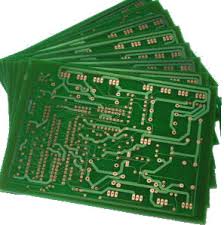
The PCB layout is a printed circuit board layout. The circuit board in the traditional process is a method of etching the circuit, so it is called a printed circuit board. With the printed board, people can avoid wiring errors during the installation process (the electronic components are connected by wires before the PCB appears, which is not only complicated and has hidden dangers). The earliest use of the PCB was in 1936 by an Austrian called Paul. Eisler, who first used on the radio. Widespread applications appeared in the 1950s.
II. Features of PCB layout
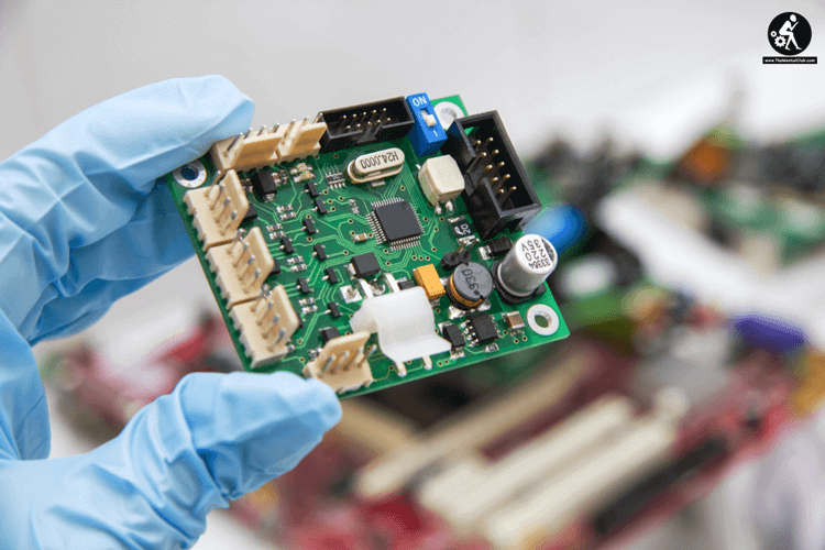
At present, the electronics industry has developed rapidly, and people’s work and life are inseparable from various electronic products. PCB, an indispensable carrier for electronic products, has also played an increasingly important role. Electronic devices are showing high performance, high speed, and thinness. PCB has become one of the most critical technologies for electronic devices as a multidisciplinary industry. The PCB industry plays a pivotal role in electronic interconnect technology.
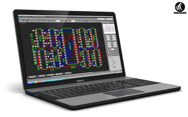
III. Process of PCB layout design
Conventional PCB design includes several steps such as building libraries, tuning netlists, layout, routing, and file output. However, the conventional PCB design process is far from meeting the increasingly complex high-speed PCB design requirements.

SI simulation, PI simulation, EMC design, and the single-board process should closely integrate into the design process. In order to achieve quality control, it is necessary to increase the evaluation process at each node, and the actual PCB design process is much more complicated.
IV. What are the common PCB layout software?
#1. Cadence Allegro
The Cadence Allegro System Interconnect Platform enables high-performance interconnects to be designed across ICs, packages and PCBs. The application platform’s collaborative design approach allows engineers to quickly optimize system interconnects between I/O buffers and across integrated circuits, packages, and PCBs. This approach avoids hardware rework and reduces hardware costs and design cycles. The constraint-driven Allegro process includes advanced features for design capture, signal integrity, and physical implementation. With its support from Cadence Encounter and the Virtuoso platform, Allegro’s collaborative design approach makes efficient design chain collaboration a reality.
#2. MentorGraphics PADS
Mentor Graphics is a leading provider of electronic design automation technology, providing complete software and hardware design solutions that enable customers to deliver powerful electronic products on the market at the lowest cost and in a short period of time. Today’s circuit boards and semiconductor components are becoming more complex. As deep submicron process technology is applied in system single-chip design, the difficulty of converting a creative idea into a product on the market has increased dramatically. This Mentor provides technologically innovative products and complete solutions that enable engineers to overcome the design challenges they face.
#3. MentorGraphics WG, EN
MentorGraphics WG, EN is a high-speed circuit simulation tool.
#4. AlTIum designer
AlTIum Designer is an integrated electronic product development system launched by Protel software developer AlTIum, which runs on the Windows operating system. The software provides designers with a new design solution that combines schematic design, circuit simulation, PCB drawing editing, topology logic auto-routing, signal integrity analysis, and design output. Designing and using this software will definitely improve the quality and efficiency of circuit design.
#5. Zuken CR
Zuken CR can understand the basic knowledge of the circuit, the principle analysis of the circuit diagram, the performance, and function of the commonly used components. It also can read the rule to make the settings.
V. Trends of PCB layout
Driven by Moore’s Law, the electronics industry is becoming more and more powerful. Today it has higher integration, faster signal speeds, and shorter and shorter product development cycles. Today electronic products are becoming miniaturized, more precise, and faster. PCB design not only needs to complete the line connection of various components but also face the challenges brought by high speed and high density.
PCB design is no longer a subsidiary of hardware development but has become an important part of “front-end IC, back-end PCB, and SE integration” in product hardware development.
The IC company not only completes the development of the chip but also gives a typical design reference. According to the functional requirements of the product, the system engineer completes the IC selection and function definition and completes the schematic diagram development by the principle of the IC company. The traditional hardware engineer circuit development work is gradually reduced, and the circuit development work is gradually turned to IC engineers and PCB engineers.
According to the principle scheme provided by the system engineer, the engineer completes the PCB design by the processing technology and capability of the current PCB factory.
If you want to learn more about PCB, check here to see more articles.


 Simply")
 – Bangla Typing Software Download")
")


")


Comments are closed.