


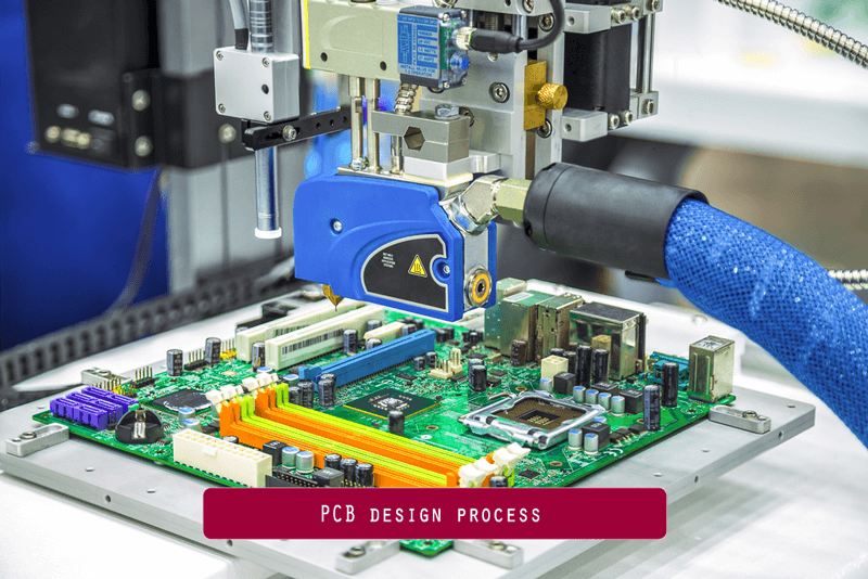
Printed circuit boards are everywhere you look but how are they made? This process is a long and hard one and it all starts out with the PCB design process. In this article, we are going to take you through the different steps that need to be followed in the PCB design process. If you’d like to find out more, make sure to read below.
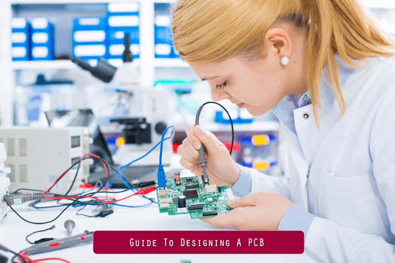
Guide To Designing A PCB
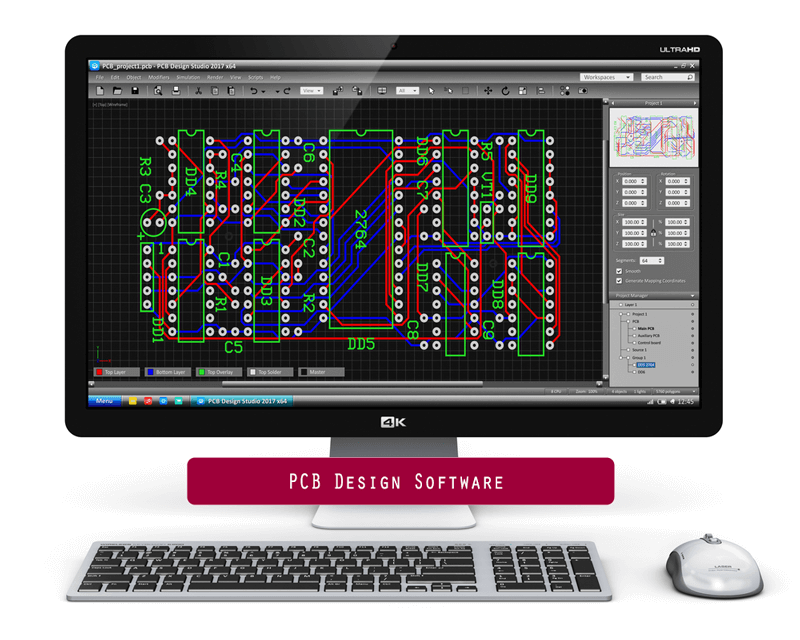
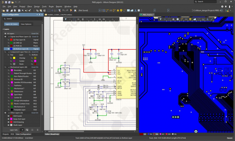
Schematic Design
The first step is to create your schematic which we suggest that you do on software like Altium. If you take a look at the top 10 PCB design software packages, then you’ll be sure to find Altium amongst others on this list. Once you have the package, you can get started on your schematic design.
Setting Up The PCB
Once your schematic is complete, you should try to create and set up the PCB. You will add details such as the shape, dimension and more if you know this information right away. Your software should help you through this process. At this point, you can also link the schematic to the PCB.
Defining The Board And Layer Stack
The next step in the process is to define the overall PCB layout including the shape and the layer stackup. The Layer Stackup Manager is the best tool that you can use to make this happen.
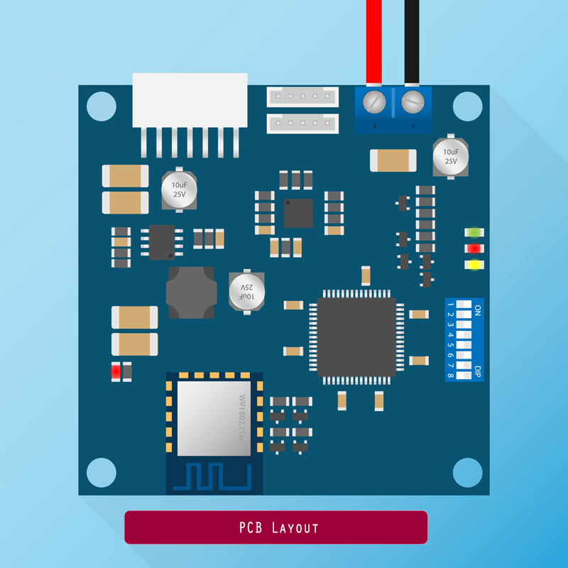
Placing Components
One of the most important parts of the PCB design process is the stage where you’ll place the components. Try to space these carefully and ensure that you are making things easier for yourself further down the line.
Inserting Drill Holes
Next, you should insert your drill holes into your design. It is advisable that you do this before you route your traces so make sure to consider this carefully.
Route Traces
When you are routing your traces, we suggest that you follow some of the routing guidelines. You should find information about this online so make sure to have a look to ensure everything goes smoothly.
Verifying PCB Layout
The next step in the process is to verify the circuit board layout. To do this, you should run a design rule check which is also known as a DRC. You can choose the rules that are relevant from a drop-down list.
Adding Labels
Once you have verified the layout, you can go ahead with adding the labels. These are very important as they will help the manufacturer when they need to understand the overall layout.
Generating Files
The final stage in this process is generating the files. Most manufacturers require that your files are saved in Gerber format, but this is not always possible in some PCB design packages. We suggest that you have a look at how you can convert these files.
Now that you understand all of the different stages of PCB design, you can go ahead and make your own printed circuit board. Remember that all of the steps are very important.


")


 – Bangla Typing Software Download")
")


![Illustrator-CC-[2017]-Full](https://thementalclub.com/wp-content/uploads/2017/05/Illustrator-CC-2017-Full-100x70.png "Illustrator CC [2017] One-on-One: Fundamentals | Tutorials [Downloadable HD Formatted Video Series – Learn Step By Step]")

